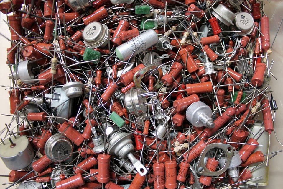
Resistor manufacturing is a promising area in the electrical industry due to the active use of these elements in the field of electronic engineering and radio electronics. In circuits of electronic and radioelectronic equipment, resistors can make up to 50% of the components used. Moreover, up to 40% of them are non-wirewound types of resistors. The quality and reliability of the equipment operation largely depends on those.
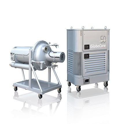
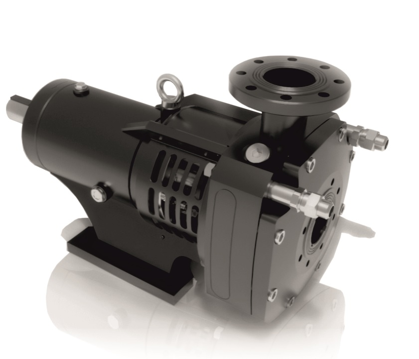
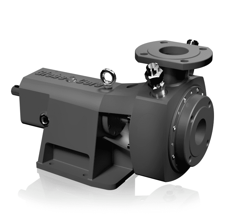
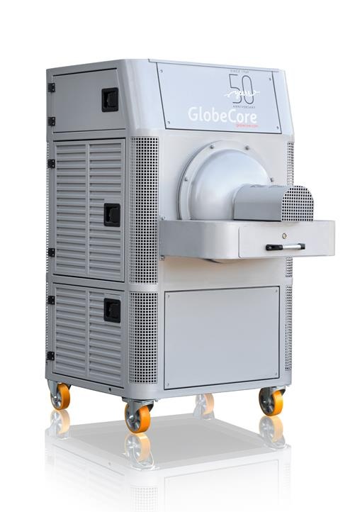
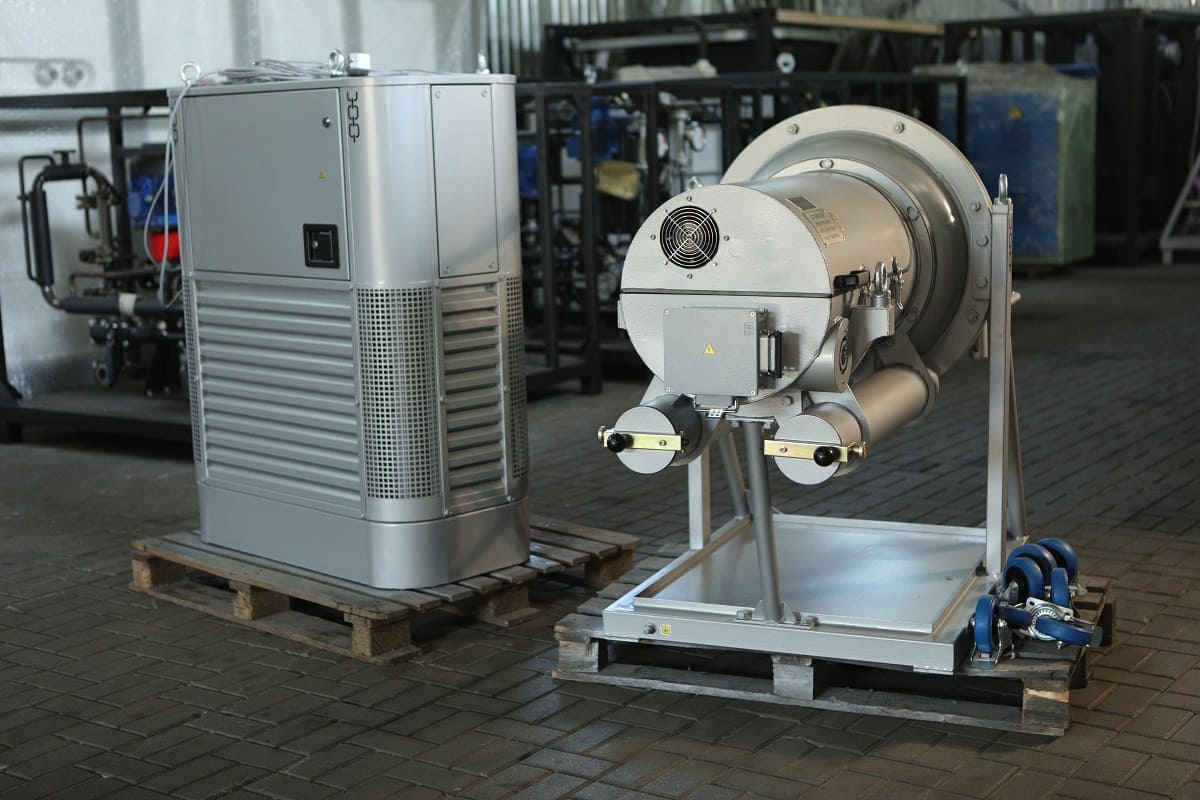
It is the manufacture of non-wirewound composite resistors during which GlobeCore vortex layer device (AVS) can be used. AVSp-150 model is suitable for this technological process.
Conventional resistor manufacturing technologies —testing results and disadvantages
Conventional resistor manufacturing in accordance with controlled parameters is distinguished by a great number of flaws due to high quality requirements, dispersion of ground and mixed components. The quality control takes into account the electromotive force (EMF) of inherent noise, the running smoothness, the temperature coefficient, and other parameters.
In order to minimize the number of flaws and to improve the quality of products, the periods of processing, grinding, and mixing the components of composite mixtures are increased. An ethyl alcohol medium is used for grinding. The material processing period can exceed two days, and the technological process generally takes more than 100 hours including the related tasks.
Ball mills are mainly used, and sometimes vibration mills are engaged as well on classic lines for resistor manufacturing from composite materials. Their efficiency can be analyzed by comparing the processing results with the indicators that were achieved by means of AVS.
Ball mills — grinding a compound based on alloyed indium oxide
In the first case, a mixture based on alloyed indium oxide was used for the study. A conventional grinding process was carried out in a mill with ultra-strong alundum balls and ceramic coating of the operating chamber. The following results were obtained (Table 1):
Table 1
| Processing time, h | Average resistance indicator of current-carrying element (R), kOhm | Average EMF of noise, μV/ V |
| 0 | 230 | 7.7 |
| 3 | 135 | 7.0 |
| 6 ≥ | 176 | 6.0 |
| 9 ≥ | 105 | 6.5 |
| 15 ≥ | 200 | 7.5 |
| 24 ≥ | 190 | 6.4 |
For comparison, when processing the compound in AVS for just 7 minutes, the average resistance indicator of the conductive element increased to 3,500 kOhm, and the EMF of noise decreased to 1.7 μV / V. This indicates the low efficiency of ball mills in the manufacture of composite resistors compared to AVS.
The duration of processing in a conventional mill has almost no effect on the quality of conductive elements. After all, AVS makes it possible to effectively increase the rated resistance indicator and to reduce the EMF of noise. It is achieved by fine grinding to the rate of 7,500 cm2/g and activation of material particles.
Ball mills – grinding a compound based on alloyed tin dioxide
The systems based on alloyed tin dioxide were subjected to processing as part of the next study. The compound was processed in a ball mill and in AVS. The results are shown in Table 2:
Table 2
| Unit | Processing time | Specific surface area, cm2/g | Average resistance indicator of current-carrying element (R), kOhm | Average indicator of temperature coefficient of resistance (TCR) 10-4, К-1, at 200ºС |
Average EMF value of noise, μV/ V |
| AVS | 0 | 2,900 | 1,300 | -11.9 | 5.3 |
| 4 min | 6,500 | 1,500 | -11.8 | 3.9 | |
| 9 min | 9,700 | 2,500 | -12.5 | 3.2 | |
| Ball mill | 0 | 4,800 | 300 | – | – |
| 3 h | 5,900 | 370 | -13.2 | 7.3 | |
| 6 h | – | 440 | -13.2 | 4.0 | |
| 9 h | 6,900 | 340 | -13.2 | 3.1 | |
| 15 h | 6,970 | 900 | -13.4 | 2.3 | |
| 24 h | 7,080 | 840 | -13.3 | 3.0 |
As you can see, the results are consistent with the same trend as in the previous study. If the maximum value of the specific surface area and the minimum EMF are observed in AVS after processing for 7 minutes, then it takes 15 hours in a ball mill. At the same time, the highest dispersion ability of particles and homogeneity of mixtures are noted.
Note that processing the compound in AVS just during 4 minutes makes it possible to obtain a material with the average resistance indicator 3–4 times higher than in the event of its grinding in a ball mill for 9 hours. This indicates the high efficiency of AVS compared to a conventional mill.
Thus, the main disadvantages of resistor manufacturing in conventional ball mills include:
- duration of processing the compounds;
- high indicators of the EMF of noise;
- high electricity consumption;
- not the best quality of grinding and mixing the components;
- low homogeneity which entails a great variance of magnetic parameters.
GlobeCore vortex layer device allows solving these problems of conventional methods for resistor manufacturing.
Resistor manufacturing through the use of a vortex layer device
Resistor manufacturing by means of a vortex layer device involves processing a composite mixture in an electromagnetic field through the use of ferromagnetic particles.
How does it work?
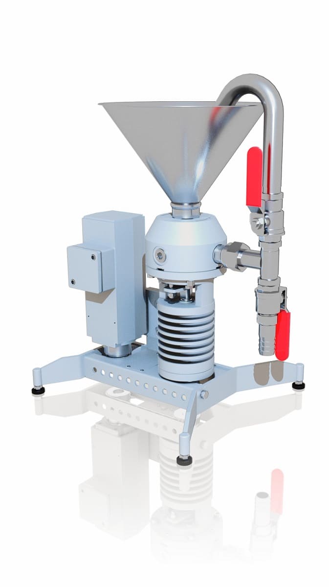
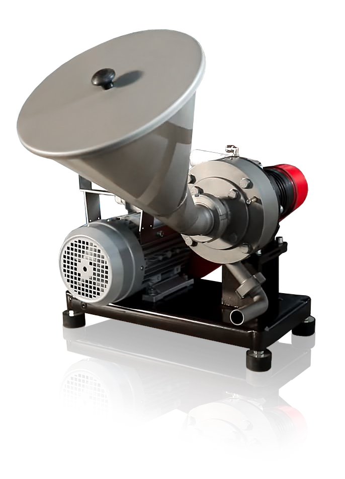
The inductor creates an electromagnetic field in the chamber under the influence of which the ferromagnetic needles and the processed material begin to move through the container.
Ferromagnetic particles collide with the substance, with one another, hit against the chamber walls, and rotate intensively — a vortex layer is generated. The dispersion and mixing processes driven by electromagnetic processing, high local pressures, acoustic vibrations, and electrolysis are observed therein. Additional processing stems from the fact that AVSp-150 model includes a reciprocation chamber which allows grinding and mixing the materials more thoroughly.
As a result, we obtain a composite mixture of finely dispersed materials on the basis of which high-quality non-wirewound resistors are further manufactured.
Results of studies
In order to determine the efficiency of grinding and mixing the compound, a system based on ZrWC and glassy bond was used. Processing was carried out during different periods of time, and the results are shown in Table 3:
Table 3
| Processing time, min | Specific surface area, cm2/g | Average particle size, µm |
| 0 | 1,150 | 5.5 |
| 2 | 2,700 | 2.36 |
| 4 | 2,120 | 2.25 |
| 6 | 2,150 | 2.97 |
| 8 | 2,140 | 2.28 |
| 12 | 1,940 | 3.29 |
We can see that the powder has the largest specific surface area after processing for 2–4 minutes. Further processing leads to the bonding of particles. The substance is ground and aggregates at the same time.
When studying the resistance rating values, it was revealed that the resistors made from powders ground to the most finely dispersed state had maximum resistance indicators. Thus, the higher the grinding fineness is, the greater the resistance will be. It is plain and simple to change this parameter in AVS — it is sufficient to change the material processing time.
Moreover, in resistor manufacturing by means of a vortex layer device, it is quite easy to monitor and control other parameters of these products — the TCR and the electromotive force of noise. For this purpose, the material processing time is changed as well. The relationship of the TCR and the duration of processing the compounds with different content of ZrWC conductive phase is shown in Table 4:
Table 4
| Processing time, min | TCR 10-6, К-2 value at +200ºС, with ZrWC content, % | |||||
| 45 | 50 | 55 | 60 | 65 | 70 | |
| 28 | 24 | 21 | 15 | 14 | 14 | |
| 2 | 25 | 24 | 18 | 17 | 16 | 16 |
| 4 | 29 | 21 | 20 | 16 | 17 | 16 |
| 6 | 20 | 17 | 18 | 15 | 15 | 16 |
| 8 | 21 | 20 | 17 | 14 | 14 | 15 |
| 12 | 24 | 19 | 16 | 14 | 14 | 11 |
Table 5 below shows the relationship of the EMF value of noise in resistors with ZrWC 45% and the compound processing time in a vortex layer device:
Table 5
| Processing time, min | 2 | 4 | 8 | 12 |
|
EMF of noise, μV/ V |
20 | 10 | 7 | 13 |
Thus, in order to manufacture resistors with certain specifications by means of AVS, it is sufficient to change two parameters — the conductive phase content and the compound processing time.
Advantages of the resistor manufacturing technology using a vortex layer device
AVS allows optimizing and intensifying the resistor manufacturing process due to the following advantages:
- Reduced compound processing time
Preparing a finely dispersed composite powder takes only a few minutes instead of tens of hours which is observed on conventional manufacturing lines. The manufacturing speed increases 50–150 times.
- Simplified manufacturing line
A number of secondary tasks and processes become unnecessary due to which resistor manufacturing becomes simpler, more affordable and advantageous.
- Cost-effectiveness
The consumption of electricity, time, and other resources when using a vortex layer device is reduced tenfold compared to the use of conventional ball or vibration units.
- Compactness
The unit weighs 560 kg. It does not take up much space — it is 1.9 meters high, 1 meter wide, and 1.5 meters long. It easily moves on wheels. It requires no pedestal or additional structures. It is much easier to use compared to classic equipment.
In addition, the technology offers opportunities for creating new types of resistors. Thus, AVSp-150 vortex layer device is highly efficient equipment with a sufficient capacity to arrange both a compact facility and a large enterprise for manufacturing electrical products. For getting advice and ordering the unit, please contact GlobeCore sales representatives.